A few weeks ago, I was reading about chip design and learned that Google switched to TSMC's 3nm process for the Pixel 10. This sparked my curiosity about what these nm processes mean, how chips are built, and the physics driving them. I also wondered about Moore's Law—the idea that transistor counts double every two years—and why it might soon hit its limits. This blog aims to explain it all in a simple way.
Exploring Today's Leading Chips: The Power and Efficiency of 3nm Technology, Built with EUV Lithography
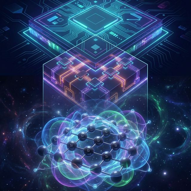
As of September 2025, the most powerful chips in wide use for smartphones and other devices are built on the 3nm process. This includes Apple's A19 Pro in the latest iPhones, Tensor G5 in Pixels, Qualcomm's Snapdragon 8 Elite Gen 5 in flagship Android phones like upcoming Samsung and Oneplus models, MediaTek's Dimensity 9500 in mid-to-high-end devices, and even Xiaomi's new XRING O1 SoC. These chips power over 80% of top smartphones, helping with tasks like taking high-quality photos, running complex games, and handling AI features without draining the battery too fast. Major makers like TSMC, Samsung, and Intel produce them, often packing around 30 billion transistors per chip—tiny switches that act like the building blocks of computation.
What makes these 3nm chips so powerful and efficient? The key is the smaller size of the transistors. At 3nm, engineers can fit more transistors into the same space compared to older 5nm or 7nm chips. This higher density lets the chip handle more work at once, like processing multiple AI tasks or rendering graphics in real time. For example, TSMC's 3nm process can make chips run 10–15% faster at the same power level, or use 25–30% less power for the same speed. That means smoother performance in apps, longer battery life, and better handling of heat. Plus, with features like advanced neural processing units (NPUs), these chips excel at on-device AI, such as real-time photo editing or voice recognition, without needing cloud help. In short, smaller transistors mean quicker electron flow, less energy waste, and more room for innovation—turning your phone into a pocket-sized powerhouse.
How are these chips built? The process begins with photolithography, where light is used to "print" tiny patterns onto thin silicon wafers, like drawing a super-detailed blueprint with light instead of ink. But at 3nm—the width of just a few dozen atoms—regular light won't cut it because the wavelengths are too long to create such fine details. That's why they turn to EUV, or Extreme Ultraviolet Lithography, a cutting-edge technique that uses much shorter light waves.
EUV works with light at a wavelength of 13.5 nanometers, which is short enough to etch features as tiny as 3nm. To generate this light, powerful lasers blast microscopic droplets of molten tin inside a vacuum chamber, creating a super-hot plasma that emits EUV photons. These photons bounce off a series of ultra-precise mirrors (up to 10 or more, coated with special layers to reflect the light without absorbing it) to focus the beam. The light then passes through a "mask" that holds the chip's design pattern, projecting it onto a wafer coated with a light-sensitive chemical called photoresist. After exposure, the wafer is developed, etched with chemicals to carve out the patterns, and layered with metals and insulators—repeating this dozens of times to build the full chip. The result? A chip that's about 30% more power-efficient than 5nm ones.
For a deeper look at EUV machines, which are mostly made by ASML, check out their official page on EUV lithography systems for an overview of the tech. If you want to see a diagram of the main components—like the light source, mirrors, and projection system—here's a detailed schematic from a research paper. These machines are marvels of engineering, each costing hundreds of millions and filling a room, but they make the impossible routine.
Advancing to 2nm: The Latest Progress, Performance Gains, and Engineering Breakthroughs Required
As of late September 2025, the shift to 2nm chips is well underway, marking a major step in making devices even more capable and energy-smart. TSMC kicked off risk production in July 2024 and is now ramping up for full mass production in the second half of this year, with early tape-outs already done—MediaTek just completed its first 2nm design on September 16, and Apple is gearing up for A20 chips in iPhones, M6 for Macs, and R2 for other gear. Nvidia and AMD are also early adopters, especially for high-performance computing like AI servers. Samsung is on a similar timeline with its SF2 2nm process, having signed deals like one with DEEPX in August for low-power AI chips. Intel's 18A node—roughly equivalent to 1.8nm—is set for volume production in the second half of 2025 too, and it's already tapped for Ericsson's 5G chips. While no phones shipped with 2nm in 2025 yet (most stuck to enhanced 3nm like Apple's N3P), expect them in 2026 flagships. Yields for TSMC are holding steady around 65% and climbing as they iron out defects.
What makes 2nm chips a big upgrade over 3nm? The smaller scale allows for even denser packing of transistors—up to 500 million per square millimeter—leading to noticeable boosts in speed and efficiency. Compared to TSMC's 3nm (N3E), 2nm can deliver 10–15% higher performance at the same power level, or cut power use by 25–30% for the same tasks, with some reports hitting up to 35% better energy savings. This means faster AI processing on your phone without extra heat, longer battery life for laptops, and more efficient data centers that sip less electricity. For instance, in gaming or video editing, you'd see smoother frames and quicker renders; in AI, it handles bigger models locally. Overall, it's about squeezing more work from less energy, keeping devices cool and portable while pushing computational limits.
So, what does it really take to reach 2nm? Building these chips demands upgrades across the board, starting with lithography. Standard EUV isn't sharp enough anymore, so they rely on High-NA EUV tools from ASML—these have a higher numerical aperture (like a better camera lens) to focus light more tightly, enabling patterns down to 2nm without blurring. On the transistor front, they're ditching FinFET designs for GAAFETs (Gate-All-Around Field-Effect Transistors), where the gate fully encircles the channel like a snug ring. This gives tighter control over electron flow, reducing leaks and boosting drive current for speed. Materials play a huge role too: Interconnects switch to low-resistance metals like cobalt or ruthenium to fight signal slowdowns, and backside power delivery (like Intel's PowerVia) routes power from the chip's rear, freeing up the front for more logic and cutting voltage drops. The whole process repeats 100+ layers on silicon wafers, but with atomic-level precision to avoid defects.
Of course, it's not all smooth sailing—the main hurdles are stubbornly low yields (where even tiny flaws scrap whole batches) and skyrocketing costs, with TSMC's 2nm wafers rumored to cost 50% more than 3nm due to pricier tools and materials. Factories, or fabs, are billion-dollar behemoths, and scaling them globally (like TSMC's Arizona site) adds logistics headaches. But research is charging ahead to smooth the path. Groups like Imec are pioneering CFET (Complementary FET) designs, which stack n-type and p-type transistors vertically for double the density without widening the footprint—think of it as 3D Tetris for circuits. They're bridging nanosheet tech to CFET with innovations like outer-wall forksheet layouts, aiming for sub-2nm scalability by the late 2020s.
For more on the 2nm journey, TSMC has a solid overview of their N2 technology on their dedicated page, including how it builds on 3nm. These advancements aren't just shrinking sizes—they're unlocking a future where tech feels effortless.
Pushing the Limits to 1nm: Who's Leading the Charge, Technologies Needed, and the Pros and Cons
Reaching the 1nm process node is like trying to build a sandcastle with grains the size of a few atoms—it's incredibly challenging but thrilling to imagine. As of September 2025, a 1nm chip means features so tiny they're just a handful of atoms wide, with silicon atoms measuring about 0.2nm in diameter. This puts us right at the edge of atomic scale, where the rules of physics get tricky. The race to 1nm is on, and several key players are making strides. Imec, a leading research group in Belgium, has laid out a detailed roadmap targeting sub-1nm nodes by 2036, focusing on stacking transistors vertically to save space. Chinese researchers at Fudan University made headlines with a 1nm gate transistor using 2D materials like molybdenum disulfide (MoS2), showing it's possible to control current at such scales. TSMC is quietly exploring beyond their 2nm node, with whispers of sub-2nm prototypes in their labs. Intel's 18A process (around 1.8nm) is set for mass production by late 2025 or early 2026, and they're already eyeing 1.4nm by 2027 as a stepping stone. In South Korea, teams at KAIST and Samsung have demoed sub-1nm gates using 1D nanowires, aiming for practical use by the early 2030s. Even startups, like those at Berkeley working with carbon nanotubes, are joining the fray, pushing the boundaries of what's possible.
Why is 1nm such a big deal? The smaller size lets you pack way more transistors into a chip—potentially 10 times more than 3nm, reaching densities of 700 million transistors per square millimeter or higher. This means chips can process data much faster, making them perfect for advanced AI tasks like real-time language translation or complex simulations. They're also up to 50% more power-efficient, so your phone could last days on a single charge, and data centers could run massive AI models with less electricity. For example, a 1nm chip might handle 8K video editing or immersive VR games without breaking a sweat, all while staying cool enough to avoid throttling. It's the kind of leap that could make sci-fi gadgets—like wearable health monitors that analyze your blood in real time—feel like everyday tech.
But how do we get there? Building 1nm chips requires a complete overhaul of current methods. EUV lithography, even with High-NA upgrades, might not cut it for such tiny patterns due to light diffraction limits. Engineers are exploring alternatives like multi-beam electron beam lithography, which uses streams of electrons to draw patterns with pinpoint accuracy, though it's slower and pricier than EUV. Another option is nanoimprint lithography, where a physical mold stamps patterns onto the wafer like a high-tech cookie cutter, offering precision at lower costs but needing perfect alignment. Transistor designs also need a rethink—FinFETs and GAAFETs struggle at this scale, so options like Forksheet FETs (which stack channels more tightly) or Negative Capacitance FETs (which boost performance with ferroelectric materials) are being tested. Materials are critical too: 2D materials like MoS2 or graphene form atom-thin channels that avoid silicon's bulkiness, improving electron flow. To manage heat, which spikes as transistors shrink, cryogenic cooling systems—operating near −100°C—might be needed in fabs or even devices. Backside power delivery, already used at 2nm, will be refined to keep signals clean.
The advantages are exciting, but the challenges are daunting. Quantum tunneling is a major headache—electrons, acting like waves, can slip through barriers thinner than 1nm, causing current leaks that mess up performance or waste power. Heat density is another issue; cramming billions of transistors into a tiny area generates intense heat, potentially melting circuits or requiring bulky cooling. Costs are astronomical—building a 1nm fab could run into tens of billions, with each wafer costing thousands due to exotic materials and low yields (early 1nm yields might dip below 50%). Reliability is a concern too: at this scale, a single misplaced atom or a stray cosmic ray can flip bits, causing errors. External factors like vibrations or electromagnetic interference could also disrupt chips. Despite these hurdles, the push continues because the rewards—ultra-efficient, ultra-powerful devices—are worth it.
For a closer look at the tech, Imec's sub-1nm roadmap outlines their vision for stacking and materials. For a visual on nanoimprint lithography, check this schematic from Canon, showing how molds could replace light-based systems. The 1nm frontier isn't just about smaller chips—it's about redefining what technology can do, even as physics pushes back.
Beyond 1nm: Sub-Nanometer Possibilities, Fundamental Limits, Challenges, and Emerging Alternatives
As we approach and surpass the 1nm node, the quest for even smaller chips ventures into sub-nanometer territory—think 0.5nm or less—where features are measured in fractions of a nanometer, barely wider than a couple of atoms. This isn't just about shrinking silicon; it's about rethinking the very foundation of computing to keep performance gains rolling. Companies like IBM are pioneering vertical Tunnel Field-Effect Transistors (TFETs) aimed at 0.5nm by around 2030, which use quantum tunneling in a controlled way to switch states with ultra-low power. Meanwhile, 2D materials such as graphene or black phosphorus are being explored for stacking in 3D configurations, allowing layers of atom-thin sheets to create dense, efficient circuits. Later-stage ideas include quantum dots—tiny semiconductor particles that trap electrons for precise control—and spintronics, where data is processed using the spin of electrons rather than their charge, potentially leading to faster, cooler operations.
The potential upsides are huge: sub-nanometer chips could sip power at levels as low as attowatts per operation, enabling devices that run for weeks on tiny batteries or mimic the brain's efficiency for AI tasks like pattern recognition. Imagine a smartphone that processes complex neural networks on-device without heating up or draining fast. However, the roadblocks are steep. Quantum interference becomes a nightmare, with electron waves overlapping and canceling each other out, leading to signal errors like static on a bad phone line. Tunneling intensifies, allowing electrons to leak through barriers uncontrollably, wasting energy and causing glitches. Thermal vibrations from heat make atoms jiggle, blurring precise structures, while manufacturing demands near-perfect control—error rates must drop below one in a trillion to avoid cascading failures. Solutions might include operating at cryogenic temperatures (near −200°C) to calm those vibrations, AI-driven "smart" factories that self-correct defects in real time, and novel materials that manipulate both light and electrons for better stability. Costs could soar into the trillions for fabs, raising questions about accessibility and who gets to control such powerful tech.
Pushing deeper reveals the ultimate wall: the smallest practical transistor size hovers between 0.3nm and 1nm, rooted in quantum mechanics and atomic physics. Silicon atoms have a diameter of about 0.22nm, so below 1nm, you're cramming components into spaces with room for just one or two atoms—leaving little margin for error. Quantum tunneling dominates here, as electrons behave like probabilistic waves rather than solid particles, slipping through ultra-thin insulators and leaking current; at barriers under 0.5nm, this leakage can spike to 10–20%, rendering switches unreliable. Interference effects cause electron waves to destructively overlap, garbling data transmission like echoes distorting sound. Add in atomic vibrations (phonons) from ambient heat, which smear out nanoscale features, and Heisenberg's uncertainty principle, which limits how precisely we can pin down an electron's position and momentum simultaneously, and control becomes impossible. Labs have demonstrated single-atom transistors, like those using phosphorus in silicon, but they only function at near-absolute zero temperatures to suppress noise. Below 0.3nm—around the size of a hafnium atom—electrons can't be confined without quantum rebellion, leading to constant errors and inefficiency. This isn't a hard stop for progress, though; it's a signal to pivot from endless shrinking to smarter architectures.
Since traditional scaling hits these physical limits, researchers are exploring alternatives to boost performance without relying solely on smaller transistors. One key approach is 3D chip stacking and chiplets, where multiple dies are layered vertically or connected horizontally, increasing density and speed through shorter interconnects—think of it as building a high-rise instead of sprawling out. Apple's rumored use of 3D stacking in 2025 MacBooks and MIT's seamless stacking techniques exemplify this, potentially cutting power use by 20–30% while enhancing multi-core efficiency. For a deep dive, check TSMC's SoIC 3D stacking overview.
Materials innovation is another frontier. Graphene, a single layer of carbon atoms, promises transistors that run at terahertz speeds with minimal heat—Georgia Tech's 2025 breakthroughs in bandgap-engineered graphene FETs could replace silicon in high-frequency apps. See Graphene-Info's transistor tag for updates. Carbon nanotubes (CNTs), tubular carbon structures, offer similar perks; recent Northwestern research highlights their stability for next-gen logic, with potential 10× efficiency gains. Explore IEEE Spectrum's CNT article. Other 2D materials like transition metal dichalcogenides (TMDs, e.g., MoS2) are gaining traction for sub-1nm scaling. Link: ACS Nano on TMDs.
State-of-the-art paradigms shift computing itself. Spintronics leverages electron spin for data storage and logic, slashing power by 100× in neuromorphic setups—Nature's 2025 review on spintronic memristors covers devices like magnetic tunnel junctions. Dive into Nature's spintronics article. Quantum dot transistors, using nanoscale particles for single-electron control, could enable flexible, low-power electronics. Link: Nature on quantum dot transistors. Optical computing swaps electrons for light, boosting speed for AI data centers. Check Future Markets' optical computing report. Finally, neuromorphic computing mimics brain neurons for efficient, adaptive processing—Intel's Loihi and BrainChip's Akida are 2025 leaders. Explore IEEE's neuromorphic feature. These paths, often combined (e.g., spintronic neuromorphics), ensure computing evolves even as scaling slows.